


Research Development

UKAM Industrial Superhard Tools has over 50 years of experience in manufacturing, research, and development. We are at the forefront of technology and are constantly engaged in Research & Development. Following the belief: "There is always room for improvement" We continue to raise standards for the whole industry.
The field of technology is in a constant state of evolution.
Our clients are demanding longer tool life, better surface finish, and tolerances. Always pushing the boundaries of what is possible. What once seemed a figment of the imagination is now, a standard routine.
Although many companies produce tools, only a select few possess the necessary equipment, personnel, and expertise to manufacture products tailored for specific applications & to meet these expectations.
We are constant developing new bond formulations, experimenting with various different materials. to use in our bond formulations, exploring new technologies and automation, testing and refining our products and technological process. We compliment our own internal research and development efforts through partnerships with some of the leading world renowned Universities, Research Centers and industry expert consultants
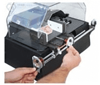
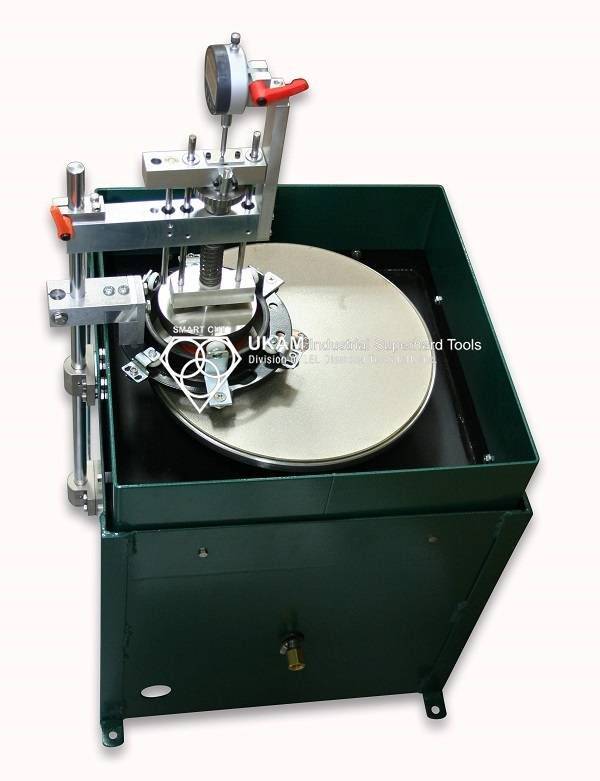
Our Experienced Engineers and Application laboratory, equipped with some of the latest Slicing, Dicing, Wafering, Drilling, & Micro Drilling Equipment is available to help you develop not only the right tools, but the Right Process for your specific Material/Application.
Working with a company that has the expertise and proven track record of producing innovative solutions for challenging slicing, dicing, drilling, grinding and polishing applications is crucial.

Count on us to help you
Stay at the forefront of technology!
We have a rich history of assisting a diverse range of clients from both industrial and R&D fields, utilizing our experience, technology, and traditions.
Here are some fields of the future and products that we are currently worked on:
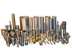
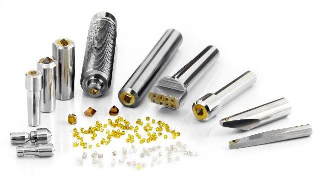
Micro Tooling & Micro Machining

The demand for smaller hole sizes and micromachining has led to technological advancements and the use of new-generation materials. Engineers are always pushing the envelope of what is possible
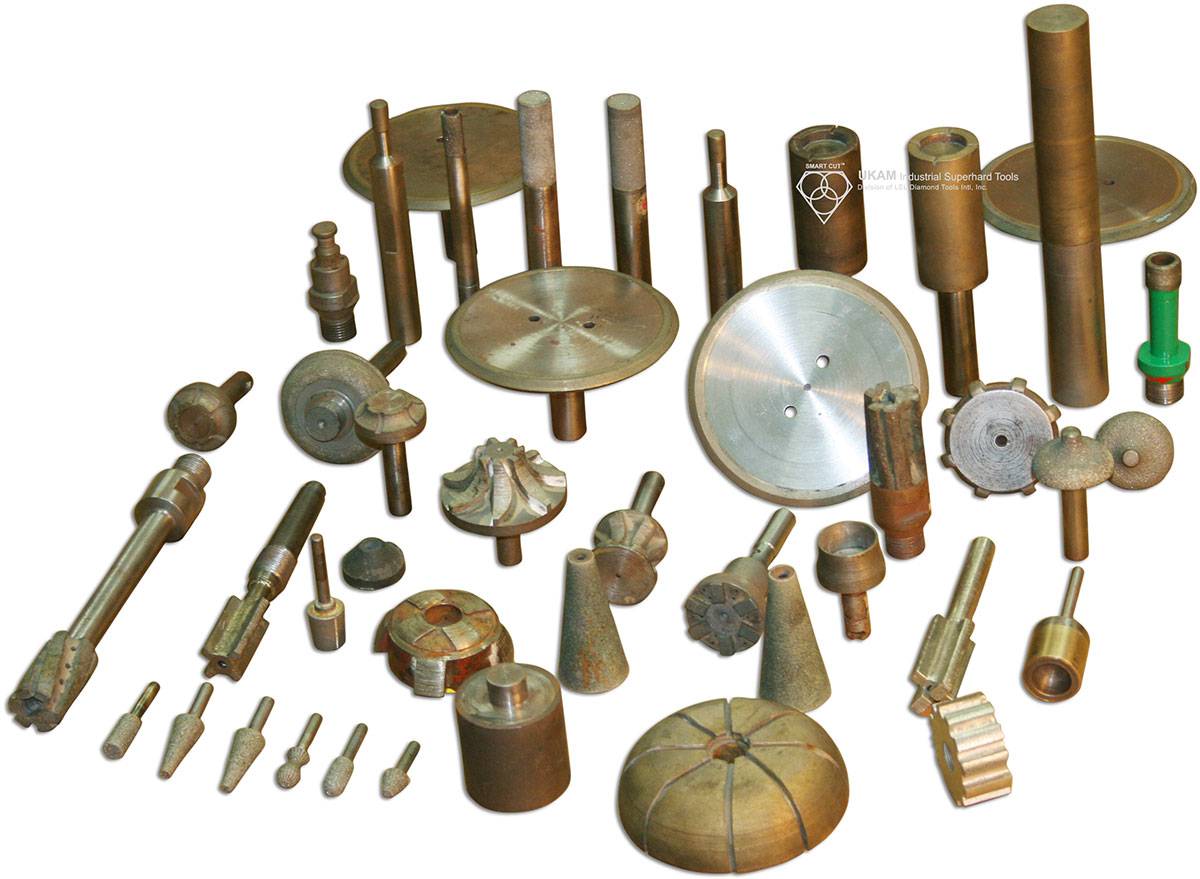
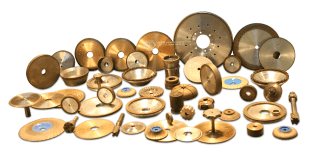
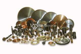
To answer this challenge, we have developed a line of standard stock and custom diamond micro tools
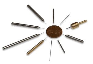
Our diamond micro drills and micro tools are used to create highly precise and complex parts and components. These tools are designed to remove material at a very fine scale and are made using a diamond plating method. Through a proprietary galvanic plating/electroplating process, diamond particles are evenly deposited on the tip over time. This unique process allows for the diamond particles to protrude from the bond matrix, resulting in a faster cutting action with minimal heat generation.


We offer a wide variety of custom diamond and CBN micro drills and tools that can be tailored to your specific requirements and drawings. High-precision tolerances are available with various head lengths, shank diameters, tip radiuses
Carbide micro tooling with or without coatings such as CVD (chemical vapor deposition) and PCD (polycrystalline diamond) is also available for certain applications, where synthetic or natural diamond is not feasible or not economical to use

New Generation & Advanced Materials
We understand the problems you are facing in machining new generation and advanced materials, and stepped up to meet this challenge by developing Precision Diamond Products and technology that will help achieve closer tolerances, faster material removal, and smoother surface finish.

The atomic structure of new generation and advanced materials is usually very different, due to their unique properties and characteristics. New generation materials are usually a composite of many other materials with possible micro and nano fillers. This creates new challenges of working with them in order to maintain best cutting speed, surface finish and minimum chipping levels
Many new generation materials are composite materials, which consist of multiple constituent materials combined at the micro or nano scale. These composites can have complex structures with different phases, reinforcing fibers or particles, and interfacial regions. Machining such materials requires considerations for the variations in hardness, toughness, and brittleness across different phases, as well as the potential for delamination or fiber/particle pullout.

Advanced materials often incorporate micro or nano-sized fillers or reinforcements to enhance their properties. Examples include carbon nanotubes, graphene, ceramic nanoparticles, or metallic whiskers. These fillers can significantly influence the mechanical behavior and machining characteristics of the material. The presence of these fillers may affect tool wear, chip formation, and surface
finish, requiring special tool designs and processes As a leader in new product development, we continue to raise standards for the whole industry.
Semiconductor / Microelectronics

Typical applications include microelectronic components, engineered ceramics, semiconductor packages, ballistic armor, electrical insulators, electronic substrates, structural components, kiln furniture, integrated circuit packages, and many others.
Semiconductor and Microelectronic
Wide range of material composition
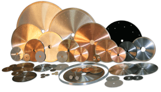
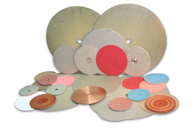
Semiconductor and microelectronic materials exhibit a wide range of properties, such as varying hardness, brittleness, and composition. Developing dicing blades and tools that can handle this variability while maintaining consistent cutting performance, while maintaining long life span and minimum chipping is challenging task
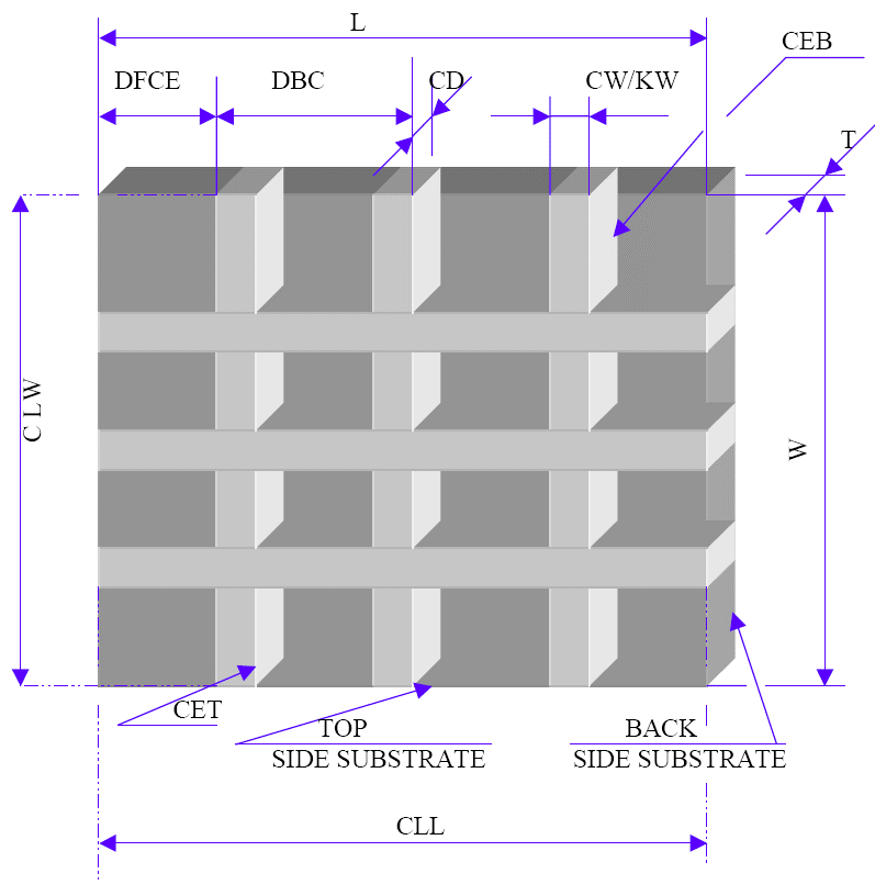
Miniaturization of components and requirements for thinner blade thicknesses
The semiconductor industry continually pushes the limits of miniaturization and utilizes advanced materials, such as compound semiconductors and stacked structures. Developing diamond dicing blades that can handle these challenging materials and meet the demands of shrinking feature


Wafer Thickness Reduction: As wafer thicknesses decrease to improve device performance, the dicing process becomes more challenging. Maintaining precise and controlled cutting to avoid wafer breakage or damage requires innovative blade designs and optimized cutting parameters.
Chip Packaging and Interconnects: With the emergence of advanced packaging technologies like fan-out wafer-level packaging (FOWLP) and 3D integration, dicing blades need to adapt to new interconnect designs, stacked structures, and non-standard wafer formats. Addressing the complexities of these packaging techniques is a challenge for blade development.